| Free Details Of How To Build A Simple Keypad-Operated Switch - Using Cheap Off-the-ShelfComponents. |
|---|
| All the information you need to build a simple keypad code-operated switch - using cheap off-the-shelf components. |
|---|
Parts List
|
|---|
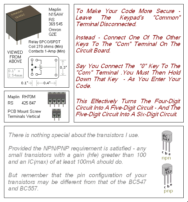
|
|
|

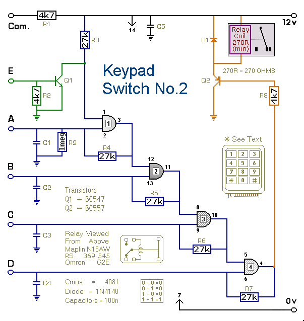
Do not use the "on-board" relay to switch mains voltage. The board's layout does not offer sufficient isolation between the relay contacts and the low-voltage components. If you want to switch mains voltage - mount a suitably rated relay somewhere safe - Away From The Board.
Construction Guide
Click here if you're new to constructing stripboard projects.
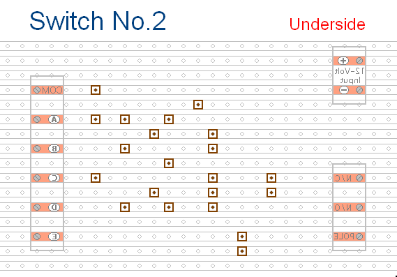
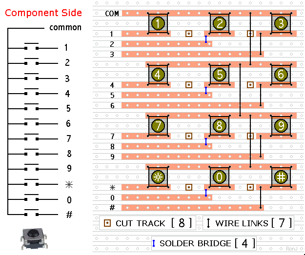
The terminals are a good set of reference points. To fit them, you may need to enlarge the holes slightly. Then turn the board over and use a felt-tip pen to mark the 21 places where the tracks are to be cut. Before you cut the tracks, use the "actual size" drawing to Check That The Pattern is Correctly Marked .
When you're satisfied that the pattern is right - cut the tracks. Make sure that the copper is cut all the way through. Sometimes a small strand of copper remains at the side of the cut and this will cause malfunction. Use a magnifying glass - and backlight the board. It only takes the smallest strand of copper to cause a problem. If you don't have the proper track-cutting tool, then a 6 to 8mm drill-bit will do. Just use the drill-bit as a hand tool - there's no need for a drilling machine.
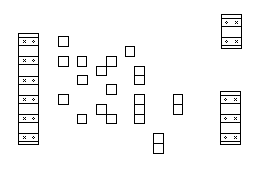
Actual Size Of Pattern
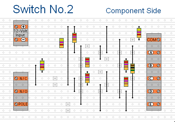
Next fit the 9 resistors and the Ten Wire Links. For the links - I used bare copper wire on the component side of the board. Telephone cable is suitable; the single stranded variety used indoors to wire telephone sockets. Stretching the core slightly will straighten it; and also allow the insulation to slip off.
The resistors are all shown lying flat on the board. However, those connected between close or adjacent tracks are mounted standing upright.
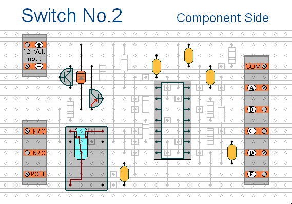
Now fit the remaining components - the diode - the two transistors - the five capacitors - the relay - and the IC socket. Note that the BC557 PNP transistor is the one drawn with a red emitter - and that the emitter is in the bottom position. If you are building the alternative version of this circuit using a BC547 NPN transistor - it should face in the opposite direction - with its emitter in the top position - similar to Q1.
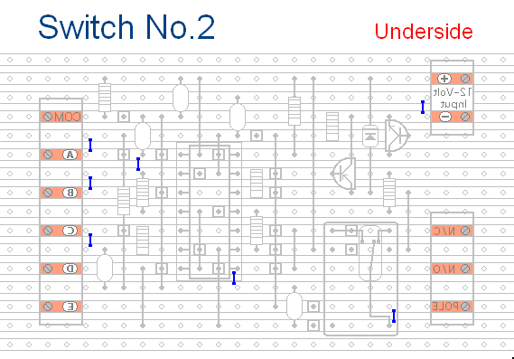
Turn the board over and examine the underside carefully - to make sure that there are no unwanted solder bridges or other connections between the tracks. If you backlight the board during the examination - it makes potential problem areas easier to spot. When you're satisfied that everything is in order - add the 7 solder bridges.
Finish off by inserting the Cmos 4081 into the socket. Pin 1 of the IC should be in the top left-hand corner. Check that all 14 pins have entered the socket. Sometimes - instead of entering the socket - a pin will curl up under the IC.
You're Now Ready To Test Your Circuit
Keypad Layout
General Information
Test Your Finished Circuit Board
|  SUGGESTIONS